Component footprints drive the PCB layout in ways you might not think. This article will describe a few examples and give suggestions on how to think about layers in a component footprint.
A footprint is composed of layers in your design tool, each of which have a defined role in describing the part on the PCB.
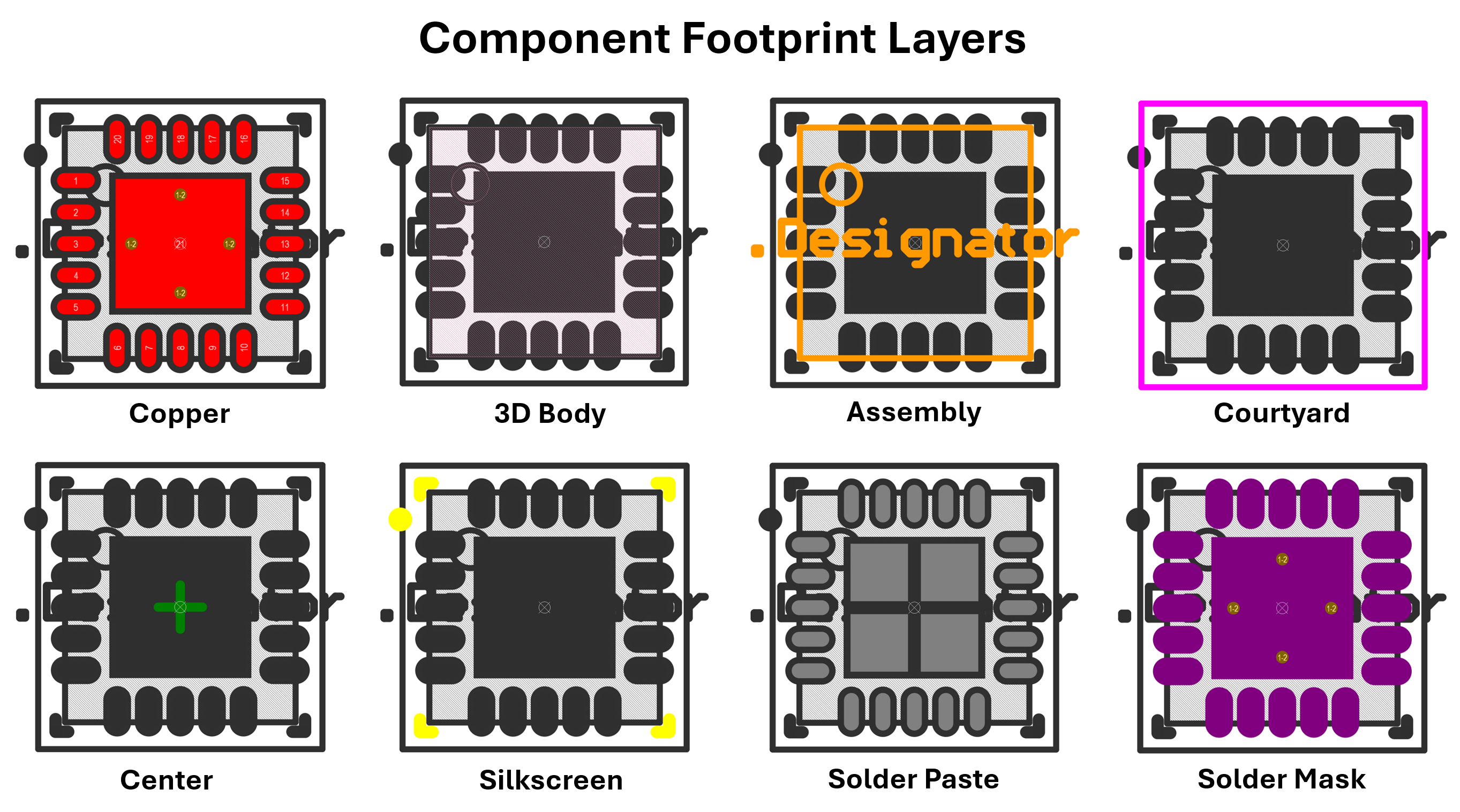
The layers of a footprint typically include:
- Component pad (SMT or multi-layer)
- Mounting holes
- Assembly information and keepout regions
- Silkscreen
- Solder paste and solder mask
- IPC courtyard
The following shows the decomposition of a typical component footprint.
One thing we see a lot of is insufficient or undefined IPC courtyards. IPC-7351 gives some guidelines on courtyard excess minimums and is helpful in preventing the PCB designer from placing components too close to one another.
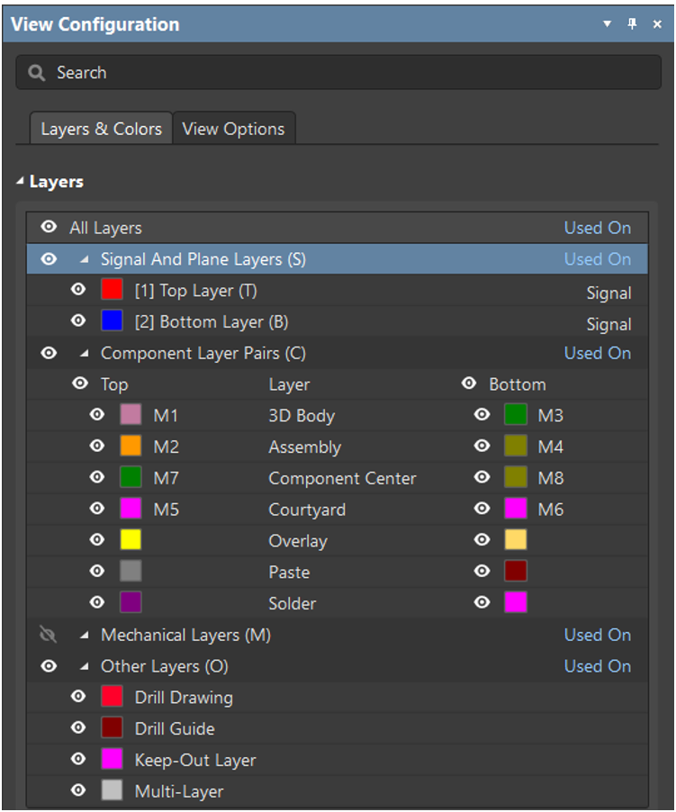
Component Layer Pairs
Specific to Altium Designer are component layer pairs, but your design tool will likely have something similar. These layer pairs are a way to translate information on one layer to another when a component is flipped from the ‘Top’ side of the board to the ‘Bottom’ side of the board.
This is useful for layers such as 3D body, assembly, and courtyard information. For example, if a component is on the top layer, its courtyard information will be on the ‘Top Courtyard’ layer. If it is flipped to the bottom layer, this information will be switched to the ‘Bottom Courtyard’ layer.
This is in contrast to Altium’s mechanical layers, which do not change layers when the component is flipped.
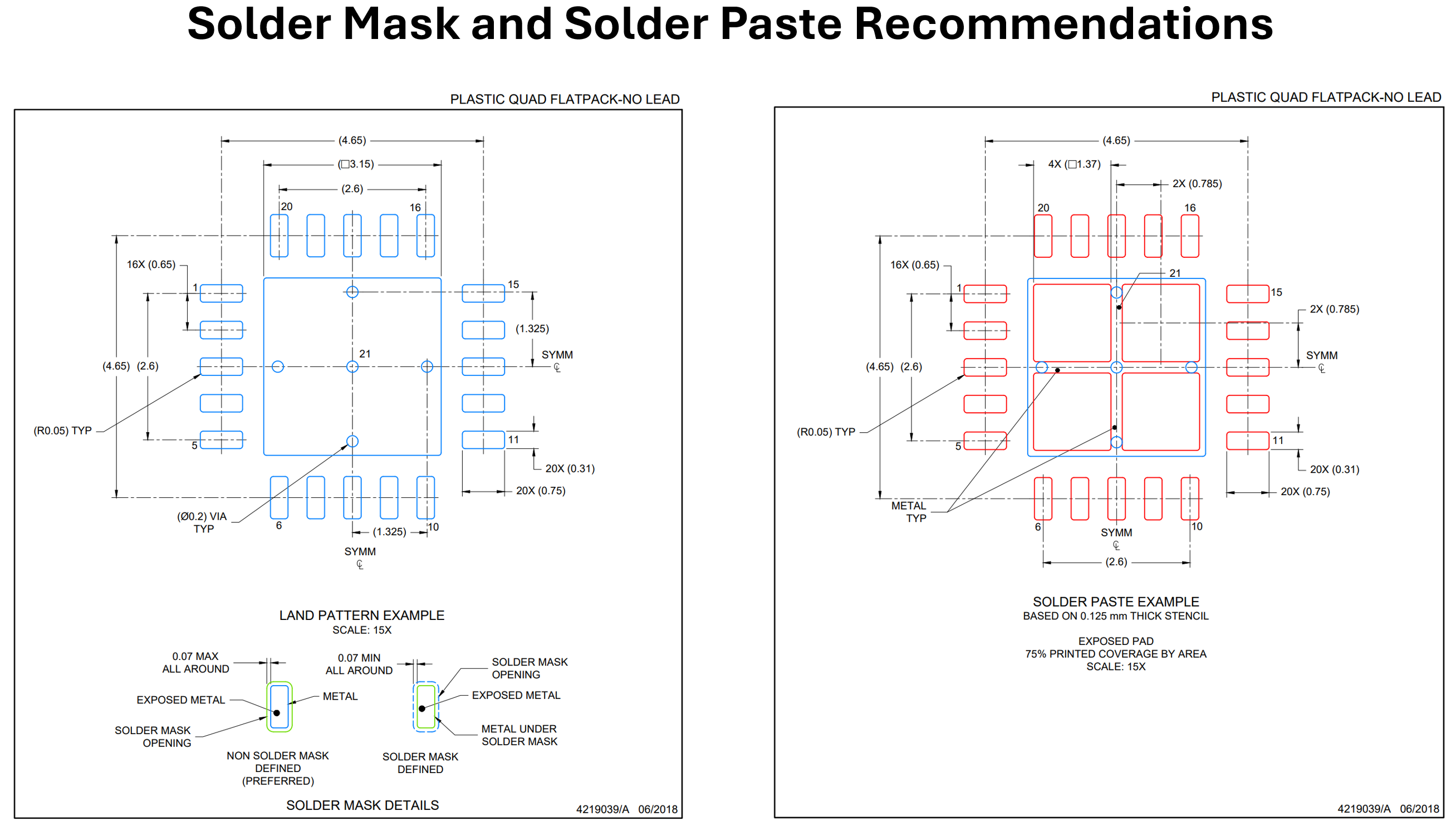
Manufacturer Recommendations
In a component datasheet, manufacturers typically recommend solder mask expansion and solder paste dimensions. These are good starting points, and are typically used for the layout unless you have manufacturing engineers that give a good reason otherwise.
One thing not related to the ECAD footprint that’s noted on the drawing below is the stencil thickness. It is often the case that an assembly house will use stencil thicknesses different than what is called out in this drawing. It can be a good exercise to know this information to see if there is excess solder or solder starvation due to solder paste volumetric changes.
Component Silkscreen to Solder Mask Clearance
When PCB manufacturers receive artwork from the customer, the files are processed to help with manufacturability. One thing manufacturers do is create a silkscreen keepout region around solder mask (usually unbeknownst to you). This prevents printing over regions without solder mask.
The following shows how this works in practice. The left image shows a pad with silkscreen clearance to solder mask expansion that is sufficient. The right image has insufficient clearance and part of the silkscreen will be removed when preparing the artwork for fabrication.
These numbers differ between manufacturers, but one way to see if this is occurring on your design is to request the processed gerbers or PDF version from your manufacturer prior to build.
In the case above, the pin 1 indicator would be impacted.
Conclusion
While this is a short list of recommendations for a footprint, this is a good starting point. The component footprint decomposition given at the beginning of the article as well as component layer pairs is a good starting point for your footprint design.
Don’t forget about manufacturer recommendations and small details like silkscreen to solder mask clearance.
Does your footprint include this information? Connect with us to get more articles like this in your feed.
Need Help With Your Project?
BuildEmber provides electronics engineering and PCB layout services for all industries. Our team has experience in power electronics, motor drives, mixed-signal, precision analog, and high-speed digital. Our team works with you to create a new design or take your existing design to the next stage of manufacturability, assembly, and reliability for mass production.
Visit us at buildember.com
Call at 832-391-5516 or email at contact@buildember.com
No responses yet