We wanted to share a few points on approaches that can be taken to reduce EMI. While this post is high level and isn’t an exhaustive list, it’s a good starting point for those trying to get a better understanding on the topic.
Switching Converter Generated EMI
Switching DC/DC converters have both high dv/dt nodes and di/dt loop areas at certain places. These are the main culprits of radiated emissions in systems. In addition to radiated emissions, switching converters operate by pulling packets of energy from the input source at a rate set by the switching frequency of the converter. A buck topology is a good example of this as it switches from drawing no load current to drawing full load current (with some inductor ripple).
For switching converters, the following are key concepts to implement in layout:
- The switch node is the high dv/dt point. The switch node should be kept as small as possible while still appropriately delivering the load current
- Use shielded inductors when your product allows (especially the kind where the leads are fully underneath the inductor)
- Always use pin 1 of an inductor on a switch node which is usually marked with a bar or dot. Pin 1 indicates where the winding of the inductor starts and the outer windings of the inductor (pin 2) shields EMI from esacping
- High di/dt loop areas should have loop areas minimized as much as possible to reduce radiated emissions
- Determine the high di/dt loop in your topology and reduce the total loop area. In a buck converter for example, the input capacitor and its connection to the freewheel diode / synchronous FET at power ground
- Use input filters on DC/DC converters to suppress conducted emissions from leaving your product or getting coupled to other nets. Place input filters close to these converters to reduce the distance these conducted emissions travel before being suppressed
- Synchronize switching converters to prevent low frequency ‘beat frequencies’ from passing through EMI filters
The following is an example of the high di/dt loop in a buck converter which is shown in red. Reducing this loop area will also reduce the ringing seen at the switch node; which will show up in EMI scans.
Image from Texas Instruments Application Note
Signal Reference and Reference Plane Transitions
With high-speed signals, one must be aware of maintaining reference plane proximity to the signal which includes proper utilization of stitching vias. Even low frequency signals can have high harmonic content due to the fast rise and fall times.
- Utilize low thickness dielectrics where possible to create a small loop area between a signal and reference plane.
- Signals with fast edge rates can encounter resonant structures such as vias stubs which radiate signals and cause signal integrity issues.
- Prioritize making via transitions from the top layer to the bottom layer on high edge-rate signal of the board when using thru vias since they don’t have stubs if possible.
- Utilize blind / buried vias to reduce stub lengths when making transitions to / from internal layers of the board
- Ensure you have proper shielding with ground pours where there are small stubs.
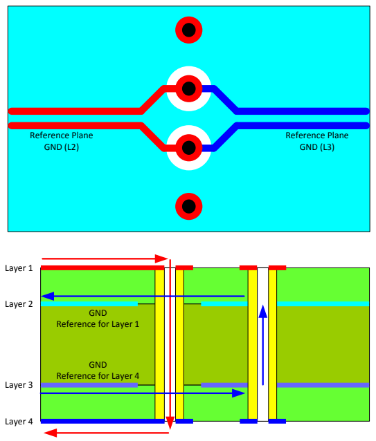
- Implement via stitching between reference planes when a transition from one layer to another also causes a change in the reference plane. Utilize two vias for differential pairs in the same fashion (show in image below).
- Signals routed over a split reference plane force return currents to take a path that’s not directly above / below. This reference discontinuity creates a larger loop area that will radiate.

Image From Toradex High-Speed Application Note
Component Breakout
The breakout of a component is important for ensuring it is properly bypassed and has termination resistors in the correct place.
- Ensure short and wide tracks going to vias when fanning out bypass capacitors. When not using via in pad, place the via as close as possible to the pad without having the via’s drill inside the soldermask opening. Placing the via inside the soldermask opening could cause solder to flow into the via and in some cases starve the solder joint.
- Via in pad using a type 7 via offers the lowest inductance without the concerns of solder leaking into the via barrel. Use more vias within reason where possible to reduce loop inductance.
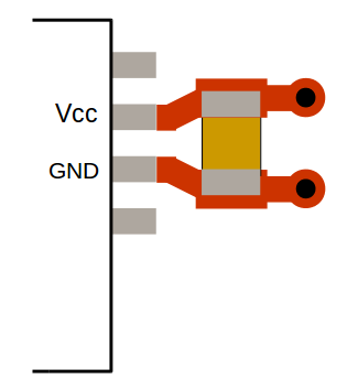
- Create small AC loop areas on decoupling capacitors to ICs (similar to power converters). The goal is to create a low inductance path to the decoupling networks.
- When the IC demands current, it sees an impedance based on how these capacitors are placed. Larger than necessary breakouts add extra inductance as seen by the IC.

Bypass capacitor with small loop area to IC
Unintended Radiators
In some cases, copper geometries and signal spacing can cause unintended radiating structures and coupling of noise. The following are a few things to keep in mind before you ship your board out for fabrication.
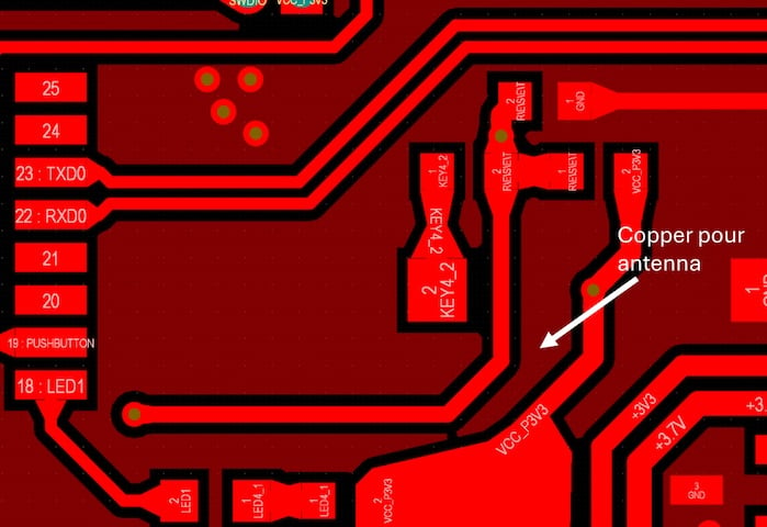
- When using copper floods, resonant structures can be formed by unterminated copper pour stubs. These pour stubs can act as antennas and radiate coupled noise. To alleviate the problem, remove or terminate the stub from your layout.
- Unintentional same net copper loops can form loop antennas that act as antennas. Break any ring structures and use a different topology for connecting nets with the same name.
- Consider common mode chokes on signals leaving your enclosure or ferrite beads to suppress high frequency content.
- Minimize crosstalk to other signals that could couple energy unwanted noise to other signals.

Unterminated copper pour causing antenna (From: All About Circuits)
Shielding
Shielding is an effective way to attenuate emissions. This can be with ground layers on a PCB or a metal shield that is mounted or soldered to the board. Some techniques for shielding include:
- Use shielding for higher frequencies to terminate electric field lines when practical
- Designs that utilize high frequency external oscillators like FPGAs and Ethernet PHYs
- Consider routing high-speed signals within inner layers so they are shielded by ground pours.
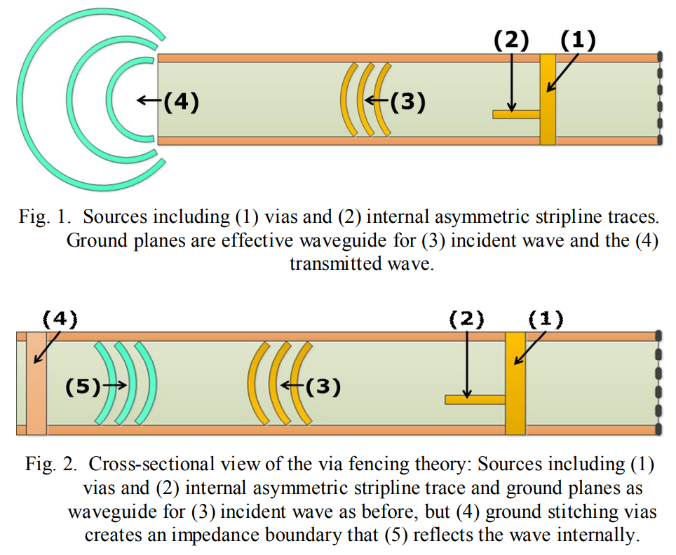
- Apply a via fence to the perimeter of you board to prevent EMI from leaking outside the edge of the PCB.
- Determine the highest frequency used on the board and harmonics where the majority of the energy content is present.
- Utilize the proper via spacing based on wavelength. This is on the order of one tenth of the wavelength for most circuits.

Via fence on PCB perimeter to prevent radiated emissions (From: North Dakota State University)
This post showcases a few of the EMI issues that we typically see at BuildEmber. However, there’s more here that we haven’t touched on due to myriad of topics that can be encountered in the world of EMI/EMC. When designing a product, it’s critical to get these problems under control since they can impact your designs performance and prevent your team from passing your EMC directives.
In future posts, we’ll dive into these topics individually and provide examples of typical problems and solutions.
Do You Need Help With Your Design?
BuildEmber has experience with PCB layout to ensure Electromagnetic Compatibility (EMC). If you have a design that you’re struggling to get compliant, or would like a second opinion on your layout, please contact us for a consultation at contact@buildember.com.

No responses yet